5.0. Overview
The diffraction simulator performs simulations of single-crystal X-ray diffraction, electron diffraction, and neutron diffraction for the crystal selected in the main window.
When X-rays are the radiation source, in addition to parallel monochromatic beams, the simulator supports precession camera and back Laue camera diffraction optics. When electrons are the radiation source, it supports selected area electron diffraction (SAED), precession electron diffraction (PED), and convergent beam electron diffraction (CBED) optics. When neutrons are the radiation source, it only supports parallel monochromatic beam diffraction optics.
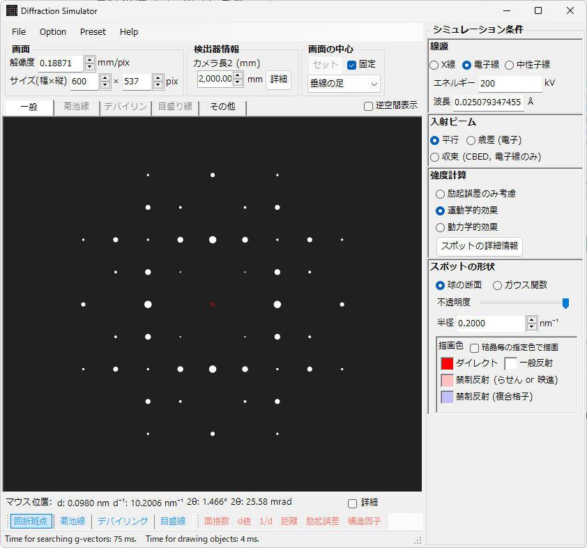
5.1. Main Drawing Area
The diffraction pattern is simulated in the area displayed in the center of the screen. By default, the direct spot is displayed as a red × mark, and the foot of the perpendicular from the detector is displayed as a green × mark. If the number of detector pixels and resolution are set, the detector range is displayed with a green frame.
The main drawing area supports the following mouse operations:
- Left drag: Rotation
- Center drag: Translation
- Right drag: Zoom in
- Right click: Zoom out
- Left double click: Display detailed information of the selected spot
Mouse Position Information
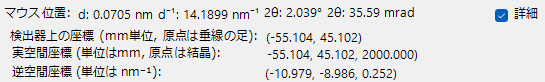
When the mouse pointer is within the main drawing area, information corresponding to that position is displayed. When “Details” is checked, the display area expands and more detailed information is shown.
5.2. File Menu
5.2.1. File
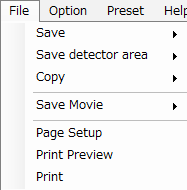
Save / Save detector area
Saves the displayed image. The latter is displayed when the number of detector pixels and resolution are set.
Save / Save detector area
Saves the displayed image. The latter is displayed when the number of detector pixels and resolution are set.
5.2.2. Preset
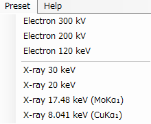
Typical incident radiation sources that are preset are displayed. Selecting one changes the incident radiation source.
5.3. Screen / Detector Information / Screen Center
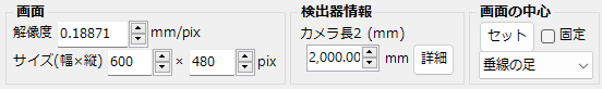
5.3.1. Screen
Resolution
Sets the length (mm) per pixel. This value is merely a matter of scale, so it does not need to be an actual value. This is a parameter that is changed by mouse zoom operations.
Size
Specifies the width and height of the drawing area in pixels. Depending on your display resolution, you may not be able to set arbitrary values.
5.3.2. Detector Information
Displays/sets the geometric positional relationship of the detector.
Camera Length 2
Displays/sets the distance from the specimen to the detector.
Details
Opens a detailed settings screen for the geometric position and resolution of the detector. For more information, see 5.8. Detector Detailed Information or A1. Definition of Coordinate System.
5.3.3. Screen Center
Sets the center of the screen. Select one of the following three options from the combo box:
- Foot of perpendicular: Sets the foot of the perpendicular from the specimen to the detector as the center of the screen.
- Direct spot: Sets the intersection point of the incident beam and the detector as the center of the screen.
- Detector center: Sets the center of the detector range as the center of the screen. The detector information must be set correctly.
Set
Pressing this button makes the center of the screen coincide with the position selected in the combo box.
Fixed
When this is checked, the center of the screen always coincides with the position selected in the combo box.
5.4. Tab Menu
5.4.1. General
Sets the color for spots, text, and other elements.
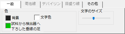
Background / Text / Foot of Perpendicular
Specifies the color for each.
Font Size
Sets the font size using the slider.
5.4.2. Kikuchi Lines
Configures settings related to Kikuchi lines. This becomes active when “Kikuchi lines” is selected in the Toolbar.
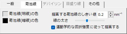
Kikuchi Line (Bright/Dark Line) Color
Specifies the color of the Kikuchi lines to be drawn. Be careful that the color does not become exactly the same as the background.
Threshold for Kikuchi Lines to be Drawn
Kikuchi lines with d values larger than this value are included in the calculation.
Line Width
Specifies the width of the Kikuchi lines.
Draw According to Kinematical Diffraction Intensity
When drawing Kikuchi lines, draw according to kinematical diffraction intensity
5.4.3. Debye Ring
This becomes active when “Debye ring” is selected in the Toolbar.
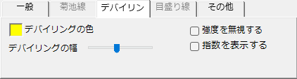
Debye Ring Color / Debye Ring Width
Specifies the color and line width of the Debye ring to be drawn.
Ignore Intensity
Draws all with the same color without considering the structure factor.
Display Indices
Displays crystal plane indices near the Debye ring.
5.4.4. Scale Lines
This becomes active when “Scale lines” is selected in the Toolbar.
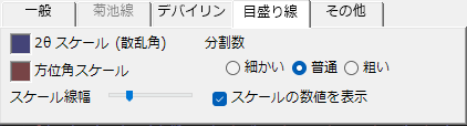
2θ Scale / Azimuthal Angle Scale
The former refers to the scattering angle direction, and the latter refers to the azimuthal angle direction. You can change the color of the scale lines for each.
Scale Line Width
Sets the thickness of the scale lines with the scale bar.
Number of Divisions
Sets the scale interval of the scale lines.
Display Scale Numeric Values
Choose whether to display labels on the scale lines.
5.4.5. Other
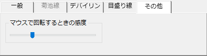
Mouse Sensitivity When Rotating
Sets the mouse sensitivity when performing mouse operations.
5.5. Simulation Conditions
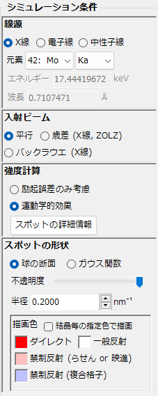
Sets the simulation conditions for calculations and display of diffraction spots. The items displayed change depending on the type of incident radiation source selected and the type of incident beam.
5.5.1. Radiation Source
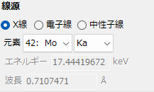
Selects the type of incident radiation source.
- X-rays: For characteristic X-rays, select the target atom and line. If you want to set an arbitrary energy/wavelength, select “0: Custom” from the combo box.
- Electrons: Set an arbitrary energy/wavelength.
- Neutrons: Set an arbitrary energy/wavelength.
5.5.2. Incident Beam
Case of X-rays
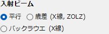
When X-rays are selected as the radiation source, the following options are displayed:
- Parallel: Performs simulation assuming finely collimated X-rays.
- Precession: Performs simulation of the diffraction pattern obtained by precessing the detector and specimen synchronously (so-called precession camera).
- Back Laue: Simulates the back Laue diffraction pattern assuming white X-rays with flat intensity in the range of 0-50 keV incident on the specimen.
Case of Electrons
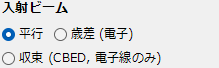
When electrons are selected as the radiation source, the following options are displayed:
- Parallel: Performs simulation assuming parallel and finely collimated electron beam. This is known as SAED (selected area electron diffraction).
- Precession: Simulates the diffraction pattern obtained by precessing the incident beam. This is known as PED (precession electron diffraction). When this mode is selected, “Intensity calculation” is automatically set to “Dynamical effect”.
- Convergence: Simulates the diffraction disks obtained by convergence with a large half-angle. This is known as CBED (convergent beam electron diffraction). When this mode is selected, “Intensity calculation” is automatically set to “Dynamical effect”, and a dedicated settings screen appears as described later in section 5.9.
Case of Neutrons
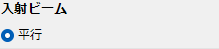
When neutrons are selected as the radiation source, only “Parallel” is displayed.
- Parallel: Performs simulation assuming finely collimated neutron beam.
5.5.3. Intensity Calculation
Selects the method for calculating the intensity of diffraction spots.
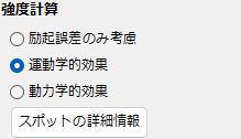
Excitation Error Only
Calculates intensity based on excitation error (distance between the Ewald sphere and the reciprocal lattice point in reciprocal space). The smaller the excitation error, the higher the intensity, with the maximum value being the “Radius” value described below. As the excitation error increases, the intensity decreases, and becomes zero when it exceeds the “Radius”.
Kinematical Effect
In addition to excitation error, calculates diffraction intensity considering the crystal structure factor.
Dynamical Effect
Calculates diffraction intensity using dynamical diffraction theory (Bloch wave method). Only selectable when electrons are chosen as the radiation source.
Spot Details
Displays detailed information about diffraction spots. See the section 5.10. Spot Details.
5.5.4. Spot Shape / Color
Sets how diffraction spots are displayed.
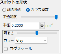
Sphere Cross-section / Gaussian Function
When sphere cross-section is selected, the simulator assumes a spherical region of reciprocal space with a certain radius centered on the reciprocal lattice point, and displays the cross-section (i.e., circle) of this sphere with the Ewald sphere as a diffraction spot. The area of the circle corresponds to the diffraction intensity.
When Gaussian function is selected, the simulator assumes a three-dimensional Gaussian function centered on the reciprocal lattice point with a certain standard deviation (\(σ\)) and a certain integrated intensity (\(I\))1, and displays the two-dimensional intensity distribution (two-dimensional Gaussian function) appearing in the cross-section of this three-dimensional Gaussian function with the Ewald sphere as a diffraction spot. The integrated intensity of the two-dimensional Gaussian function corresponds to the diffraction intensity.
Opacity
Specifies the transparency of the diffraction spots to be drawn.
Radius
Specifies a quantity corresponding to the radius of the reciprocal lattice point. The value specified here (hereinafter referred to as \(R\)) affects the display method of diffraction spots as follows, depending on the choices of “Spot shape” and “Intensity calculation”. In the following explanation, the standard deviation of the Gaussian function is denoted as \(σ\), and the “Brightness” value described below is denoted as \(B\).
| Spot Shape | Intensity Calculation | Diffraction Spot Display Method | ||
|---|---|---|---|---|
| Gaussian Function | Excitation Error Only | Assume a three-dimensional Gaussian function with \(R\) as standard deviation \(σ\) | Integrated intensity of 3D Gaussian function is \(B\) | Display the intensity distribution (2D Gaussian function) appearing in the cross-section of the 3D Gaussian function with the Ewald sphere as the diffraction spot |
| Kinematical Effect | Integrated intensity of 3D Gaussian function is \(B\) × [kinematical relative diffraction intensity] | |||
| Dynamical Effect | Assume a two-dimensional Gaussian function with \(R\) as standard deviation \(σ\) | Integrated intensity of 2D Gaussian function is \(B\) × [dynamical relative diffraction intensity] | Display the 2D Gaussian function defined on the left as the diffraction spot directly2 | |
| Sphere Cross-section | Excitation Error Only | Assume a sphere with \(R\) as radius | Display the cross-section of the sphere defined on the left with the Ewald sphere as the diffraction spot | |
| Kinematical Effect | Assume a sphere with \(R\) × [kinematical relative diffraction intensity]1/3 as radius3 | |||
| Dynamical Effect | Display a circle with radius \(R\) × [dynamical relative diffraction intensity]1/2 as the diffraction spot (circle area is proportional to dynamical relative diffraction intensity) | |||
Brightness (Only when Gaussian Function is selected)
This is the value of \(B\) mentioned above. Adjust with the scale bar.
Color (Only when Gaussian Function is selected)
Choose from Gray scale, Cold-warm color, Spectrum, or Fire.
Log Scale (Only when Gaussian Function is selected)
When checked, intensity is displayed on a log scale.
Drawing Color
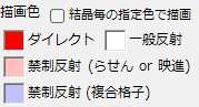
Sets the color of the diffraction spots.
Forbidden reflections are diffraction spots that should have zero intensity due to systematic absences, so this is a meaningful setting only when intensity calculation is “Excitation error only”.
5.5.5. Bloch Wave Related
Bloch Wave Settings (Only when “Electrons” + “Dynamical Effect” is selected)
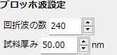
Sets the number of Bloch waves to include in dynamical diffraction intensity calculations. In the Bloch wave method, the computational cost is proportional to the cube of this number, so gradually increase it while monitoring the results.
Specimen Thickness
Sets the specimen thickness. In the Bloch wave method, specimen thickness is unrelated to calculation speed.
Precession Settings (Only when “Electrons” + “Precession” is selected)
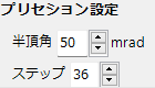
Half-angle
Sets the half-angle of the incident electrons in precession electron diffraction.
Step
Precession electron diffraction is simulated by summing parallel beam electron diffraction from multiple directions. This parameter sets the number of such directions.
5.6. Toolbar

5.6.1. Objects to Draw
Diffraction Spots
Toggles the display/hide of diffraction spots.
Kikuchi Lines
Toggles the display/hide of Kikuchi lines.
Debye Ring
Toggles the display/hide of Debye rings4.
Scale Lines
Toggles the display/hide of scale lines.
5.6.2. Display Information
Plane Indices / d value / 1/d / Excitation Error / Structure Factor
Selects the information in the labels displayed near spots.
5.7. Reciprocal Space Display
When “Reciprocal space display” at the top of the screen is checked, a window showing the relationship between the Ewald sphere and reciprocal lattice points is displayed on the right side of the main drawing area.
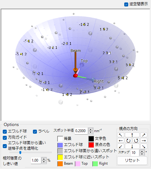
Mouse Operations
- Left drag: Rotation of viewpoint direction (not the crystal)
- Right drag (up/down): Zoom in/out
Ewald Sphere
Display/hide of the Ewald sphere
Direction Guide
Display/hide of arrows indicating incident beam, screen up direction, and screen right direction
Make Distant Reciprocal Lattice Points Transparent
Adjust with the slider
Relative Intensity Threshold
When “Kinematical effect” or “Dynamical effect” is selected in the intensity calculation, only reciprocal lattice points with relative intensity exceeding the threshold are calculated.
Spot Radius
Sets the radius of the sphere representing the reciprocal lattice point.
Color
Sets the drawing color.
Viewpoint Direction
Adjusts the viewpoint direction using arrow buttons. Pressing Reset returns to the initial state.
5.8. Detector Detailed Information
Performs detailed settings related to the detector.
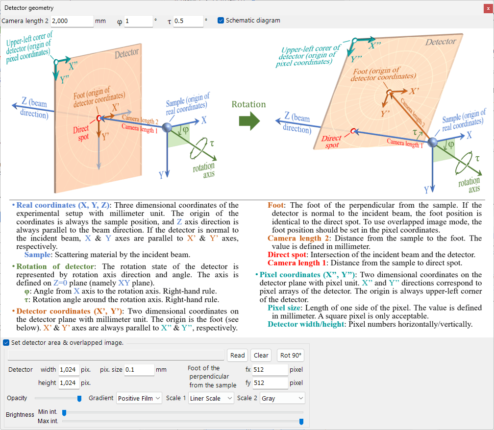
Schematic diagram
A schematic diagram explaining the meaning of the parameters is displayed. For more details, refer to A1. Definition of Coordinate System.
Set detector area & overlapped image
By setting the number of detector pixels and pixel size, you can overlay a detector image on the simulated diffraction pattern or display only the detector frame. The detector area is displayed as a green rectangle.
To overlay an image, press the Read button to load the image. Then set the pixel size and foot of perpendicular to the correct values. You can also adjust the image transparency, color scale, and brightness.
If you want to display only the detector frame, do not load an image, but set the pixel size, number of pixels, and foot of perpendicular.
5.9. CBED Settings
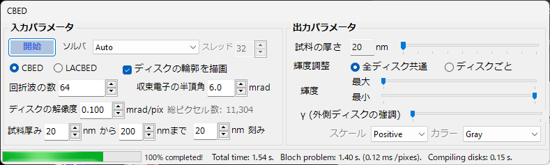
CBED is a computation that requires significant resources. Therefore, calculations are not performed in real-time. Press the “Execute” button to run the calculation.
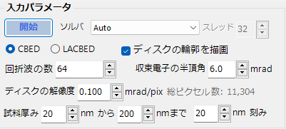
5.9.1. Input Parameters
Displays/sets various input parameters required for CBED calculation.
CBED/LACBED
Selects between normal convergent beam electron diffraction (CBED) or large-angle CBED (LACBED). The former draws all diffraction disks of interest, while the latter draws only the g=0 diffraction disk.
Solver
The Bloch wave method consumes significant resources in calculating eigenvalues and eigenvectors. You can select the algorithm (solver) to solve the eigenvalue problem from the following:
- Auto: Automatically selects the fastest from the three below.
- MKL: Uses Intel’s library MKL (https://software.intel.com/en-us/mkl).
- Eigen: Uses the open-source library Eigen (https://gitlab.com/libeigen/eigen).
- Managed: Uses the open-source library Mathnet (https://github.com/mathnet/).
Based on the author’s experience, Eigen is fastest when the number of Bloch waves is small (< ~500), and MKL is fastest when it is large (> ~500).
Number of Diffraction Waves
Specifies how many Bloch waves are included in the calculation. Computational cost is proportional to the cube of the number of Bloch waves, so entering large values will increase calculation time.
Half-angle of Convergent Electron
Specifies the convergence angle of the electron beam.
Draw Disk Outline
Displays a guide showing the size of the CBED disk in the main drawing area. Refer to this when determining the half-angle.
Disk Resolution
Specifies the resolution of the CBED disk. The disk is divided into approximately π/4 times the square of [half-angle]/[resolution] pixels. Since the number of pixels is proportional to the computational cost, reducing resolution will increase calculation time.
Specimen Thickness ## nm from ## nm to ## nm increment
Performs CBED simulation for multiple specified thicknesses. Since this software performs dynamical calculations using the Bloch wave method, the computational cost remains almost unchanged as thickness varies.
5.9.3. Output Parameters
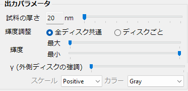
Specimen Thickness
Specifies the specimen thickness to display.
Brightness Adjustment
CBED disks sometimes show very large differences in brightness between disks. You can choose whether to perform brightness adjustment common to all disks or brightness adjustment for each disk.
Brightness
Adjust brightness with the scale bar.
γ (Outer Disk Enhancement)
This parameter enhances the brightness of disks at higher scattering angles.
Scale / Color
Sets the drawing color for CBED disks.
5.10. Diffraction Spot Details
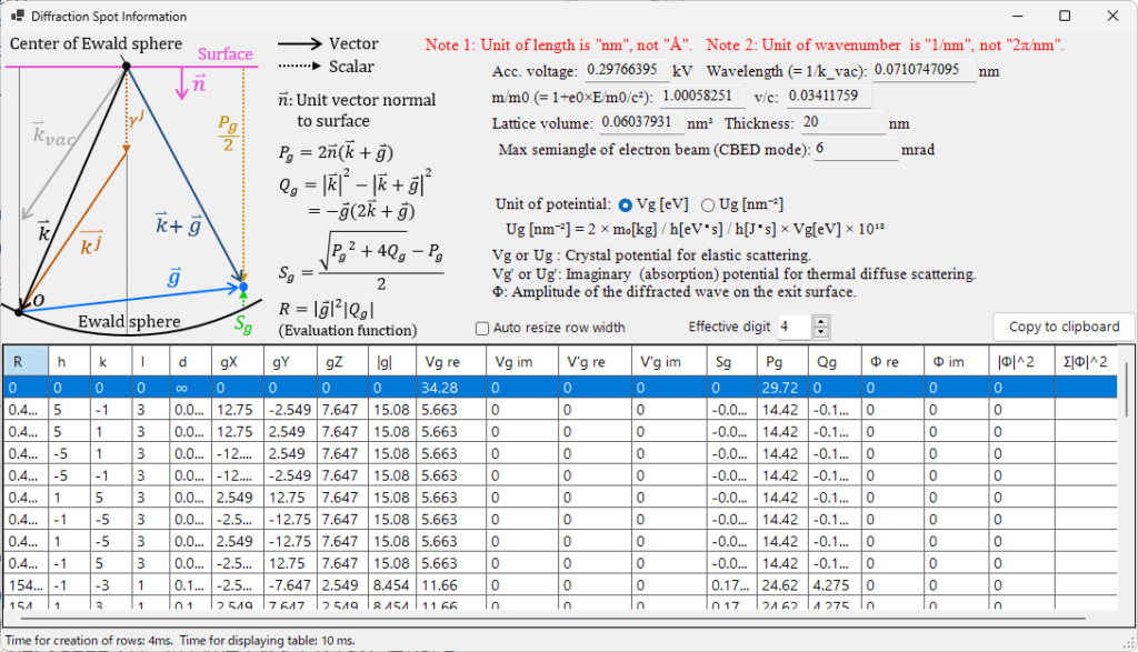
Displays detailed information about diffraction spots. Refer to the schematic diagram in the upper left for the meaning of the symbols.
Copy to clipboard
Copies the table contents to the clipboard. The format is tab-separated, which can be pasted into Excel.